Small Signal (AC) Bipolar Parameters from SPICE Parameters

Requires a Wolfram Notebook System
Interact on desktop, mobile and cloud with the free Wolfram Player or other Wolfram Language products.
This Demonstration computes a group of high-frequency bipolar junction transistor parameters (such as "ft", the unity gain bandwidth frequency) from the appropriate SPICE model parameters. The result is plotted on a graph versus either collector current (Ic) or voltage collector to emitter (Vce), whichever is relevant. It also gives a numerical result for the parameter above the graph for a particular value of Ic and Vce set by their sliders.
Contributed by: Allen Hollister (September 2009)
Open content licensed under CC BY-NC-SA
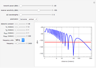
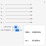
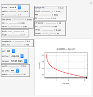
Snapshots


Details
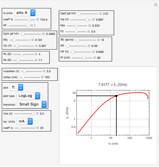
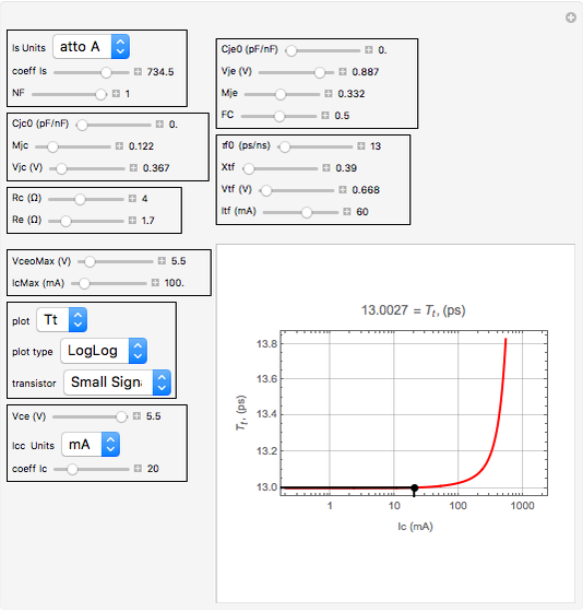
SPICE is a widely used analog simulation program. It models the Bipolar Junction Transistor (BJT) through the use of a series of model parameters that make up the Gummel–Poon physical model. Unfortunately these parameters provide little insight into the external parameters we engineers like to use to describe the device. This program inputs the relevant SPICE parameters (through the plethora of sliders) and converts them to a series of graphs and numbers for the external parameters of interest. These external parameters are: ft, Tt, Vbe, Vbc, Cjc, C , Cet, and Ct. Briefly, ft is the frequency at which unity current gain occurs. It is plotted against the collector current Ic. The ft at a particular operating point (vce, Icc) is given just above the graph. Tt is
  ; Vbe is the external node Base to Emitter voltage. It is graphed against Ic; Vbc is the Base to Collector Voltage and is plotted against vce. If Vbc is below the blue line, the device has a forwarded biased collector base junction and the device is in saturation. Cjc is the Collector Base junction capacitance and is plotted against vce (voltage collector to emitter); C is the capacitance in the linear model that exists between the base and emitter. It is equal to gm times Tt. gm is the transconductance gain and is equal to Ic/Vt where Vt is the thermal voltage and is equal to 25.8708 mv at room temperature. C is plotted against Ic. Cet is a capacitor in series with C that is present because of the emitter bulk resistance Re. Cet is equal to Tt/Re. Finally Ct is the series combination of C and Cet. If you look into the transistor when forward biased but with no emitter degeneration, this is the input capacitance you would see. The controls located above the graph are used to enter the SPICE parameters. Those controls to the left of the graph are used to set and measure the output parameters such as ft and Tt as well as vce and Icc. (I distinguish between Ic which is the
  axis parameter used for the graph, and Icc which is the collector current set by the sliders and used to calculate the location of the lines and the parameter of interest displayed directly above the graph).
The absolute maximum collector current (IcMax) and the absolute maximum collector to emitter voltage (VceoMax) are used to limit certain parameters to prevent creating a situation where the device would be operating outside its acceptable boundaries. These parameters are entered using the slider controls labeled IcMax and VceoMax respectively. Their values are usually found on the transistor data sheet. Units are mA and volts respectively.
It should be understood that while effort has been made to prevent weird results (such as imaginary values) through the use of limits, there will always be a set of parameters that will violate something. This is especially true if one is changing from one kind of transistor to another. A power transistor that can operate at 100 Amps probably doesn't have an Rc or Re values in the tens of Ohms. If it did, it would saturate for all but the highest operating voltages (producing imaginary results). So it is important to input all the relevant SPICE parameters before using any of the results. If you wish to view a parameter such as ft with a collector current (for example) that is greater than the maximum allowable current as set by the IcMax control, you will have to increase IcMax. Even with the correct parameters entered, it is possible to create combinations of Ic and Vce where, even though the parameters are within the absolute maximum values, the transistor saturates. For example, If you reduce the collector current to a very small number, then reduce Vce to the smallest number allowed by the limit at that setting, then increase the collector current, the device will saturate and the display will turn pink and display an imaginary number. Observe that the Vce control is showing pink at its lowest setting at this time indicating that for the current setting of collector current, Vce needs to be increased, Simply move the slider to the right and a new value will immediately appear and the device will go back to normal. In this case, the display will become pink indicating an error. The blue line on the Vbc plot represents saturation. Any combination of Vce and Ic that puts Vbc above this line should be OK.
In addition, other protections limit the range of Vce. For example, the Cjc plot has a limit on Vce that prevents the base collector junction from forward biasing.
The collector current (Icc) has such a large range that a control was set up to ease the data entry. Icc can range over many orders of magnitude. For this parameter, the data is entered by two separate controls. One gives a power value (defined as "units") and the other a coefficient. The value of Icc is then equal to the coefficient times  .
.
The same is true for the SPICE parameter "Is". It also has two separate controls. One is a "power" value defined as "Is units" and the other is "coeffic Is". The value of Is is the product of these two controls. Thus if one selects "Atto A" for Is units and 734.5 for coeffic Is, the value of Is will be  .
.
Again to facilitate data entry, two kinds of transistors are identified—power devices and small signal devices. This data is entered via the dropdown control labeled "transistor". When this control is set to "Small Signal", all time units are entered in ps, all capacitances in pF. Output frequencies are in GHz, output times are in ps and output capacitances are in pF. When "Power" is selected, all time units become ns and all capacitances are entered in nF. Frequency has units of MHz. The only SPICE parameters affected by "transistor" are cjeo, cjco, and τf0. In addition to the units change, the limits on the controls IcMax and VceoMax change depending on the setting of the control "transistor".
Be aware that once the data is entered under either "Small Signal" or "Power", switching between these two will change the units of cjeo, cjco, and τf0. The result will be that the graph will look the same, but the output frequencies, times, and capacitances units will have changed from GHz, ps, and pF to MHz, ns, and nF—or vice-versa, respectively.
Before entering the SPICE parameters Cjeo, Cjco, and τf0, you should first choose the setting for "transistor" as this will determine if the units for these parameters are in (pF, ps) or (nF, ns). For example, if you entered "2.5" for Cjeo, and if you did this with "Small Signal" selected, the 2.5 will be interpreted as 2.5 pF; else it will be interpreted as 2.5 nF.
All currents have units of ma except "Is" and "Icc" which has units set by the control labeled Is units and Icc units respectively. Resistance is in ohms and voltage is in volts.
If the sliders run out of range for your device, click on the + sign at the end of the slider and you can enter the number directly. If it is out of the normal bounds set by the initialization of the slider, it will show red. However it will still accept the number and do the appropriate calculation.
The example transistor used in the Demonstration is the NE851M03.
By playing with the controls, you can explore different parameters. For example, if you would like to see how τf varies with current and voltage, set Cje0 and Cjc0 to zero and select the Tt plot. Under these conditions, Tt is equal to τf. This is shown in the last snapshot.
Accuracy:
The Gummel Poon model consists of 40 different parameters—this program uses 15 of these parameters. Therefore, one can expect some error at the limits. Specifically not modeled are high-current problems (base pushout) or Kirk effect (modeled by IKF and IKR), low currents modeled by Ise, and basewidth modulation or Early and Late voltages modeled by VAf and VAR. The DC current gain is assumed infinite. However, the idea was to create something relatively simple (having 40 sliders would have been unreasonable) with a focus on high frequency performance—not so much DC effects. Certain DC parameters such as Vbe and Vbc were needed to calculate the high frequency parameters, so they are available for output, but they are not accurate over large current and voltage ranges. A second assumption is that most devices are operated near their peak performance areas (otherwise choose a different device) so the very low and high current areas do not matter as much. The program was checked against SPICE using full models for several different transistors. Errors are within a few percent if the device is operated at reasonable bias points and not at extremes (such as near saturation).
Finally, the results of this Demonstration are for the underlying device only. It does not include any stray elements such as package inductances.
References
[1] A. Hollister, Wideband Amplifier Design, Raleigh, NC: SciTech Publishing, 2007.
[2] Besser Associates Class, Wideband/HF Amplifier Design Techniques.
Permanent Citation
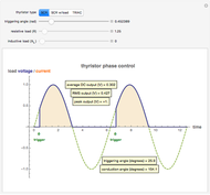 AC Thyristor Operation
Harley H. Hartman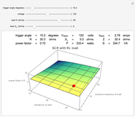 AC Thyristor Trigger Angle versus Power Factor
Harley H. Hartman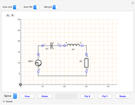 SPICE Program for Electronic Circuits
George Irwin Balanced T-Coil Parameters
Allen Hollister Frequency Response of an LCR Circuit
Contributed by: Kallol Das (St. Aloysius College, Jabalpur, India) Three-Branch Electrical Circuit
Darya Aleinikava Bifurcation Analysis of a Cubic Memristor Model
Vanessa Botta, Marcelo Messias, and Cristiane Néspoli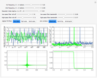 Digital Filters with Windowed Sinc Finite Impulse Response
Dana Tremblay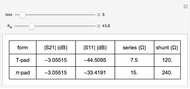 RF Attenuator T or Pi Values in 5% Resistors
Mostafa AbuShaaban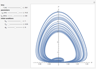 Chaotic Dynamics of a Modulated Semiconductor Laser
Manu P. John and V. M. Nandakumaran