Band Structure of P-N Junction Semiconductor

Requires a Wolfram Notebook System
Interact on desktop, mobile and cloud with the free Wolfram Player or other Wolfram Language products.
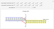
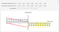
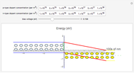
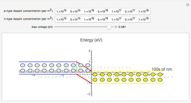
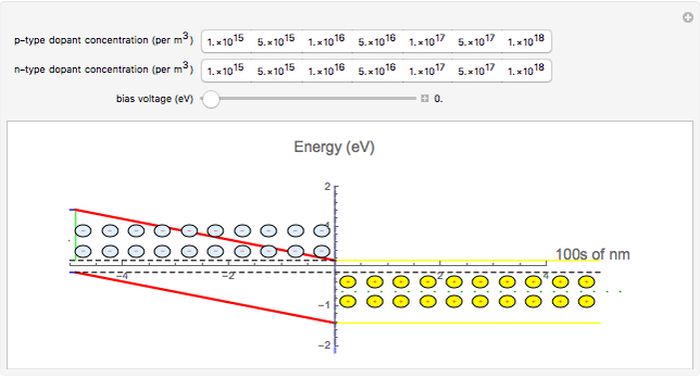
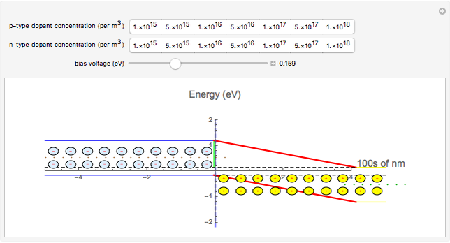
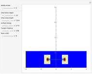
P-N Junctions are types of semiconductors with a unique band structure and are used in variety of applications from solar cells to LEDs to transistors. This Demonstration shows the electronic band structure, above, of a P-N junction as well as the physical junction, below, for a generic semiconductor. The left side, in blue, contains p-type dopant, which provides excess holes, brown circles, as the charge carriers. The right side, in yellow, contains a n-type dopant, which provides excess electrons, green circles, as the charge carriers. The dotted red line represents the Fermi level
[more]
Contributed by: Sam Shames (July 2012)
Open content licensed under CC BY-NC-SA
Snapshots
Details
A P-N junction is formed when a p-type semiconductor and an n-type semiconductor are joined with a metallurgical junction. Because of the difference in concentration of dopants on each side, there is a driving force for diffusion across the interface; excess electrons from the n side and excess holes from the p side diffuse until the chemical potential (Fermi level) is equal across both sides. This creates the bent band structure and a depletion region within the junction, an area where all the free charge carriers are depleted. Without free carriers, the ions left behind generate an electric field and a built-in voltage, creating a barrier for diffusion. Applying a forward bias voltage lowers the built-in voltage, reducing the barrier and allowing current to flow.
Based on material from Electrical, Optical, and Magnetic Properties of Materials, MIT, spring 2012, taught by Professor Polina Anikeeva.
Permanent Citation
"Band Structure of P-N Junction Semiconductor"
http://demonstrations.wolfram.com/BandStructureOfPNJunctionSemiconductor/
Wolfram Demonstrations Project
Published: July 2 2012
 Mechanism of a Solar Cell
Christopher P. Muzzillo Impedance Spectra of Piezoelectric Rods
Robert McIntosh Trace Width of a Printed Circuit Board
Josiah McClurg Electromagnetic Waves in Optical Fibers
Y. Shibuya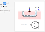 Primer on Bipolar Junction Transistors
S. M. Blinder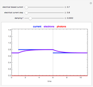 Transient Response of a Semiconductor Laser
Philippe Brosson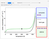 Electrical Conductivity of Silicon Semiconductors
Nathan S Nelson Electronic Band Structure of Armchair and Zigzag Graphene Nanoribbons
Jessica Alfonsi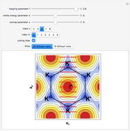 Electronic Band Structure of a Single-Walled Carbon Nanotube by the Zone-Folding Method
Jessica Alfonsi (University of Padova, Italy)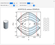 Band Structures in Zigzag Graphene Nanoribbons and Armchair Carbon Nanotubes
Vasil Saroka
-
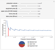
 Process-Based Cost Model for Sand-Casting Bronze Bells
Sam Shames -
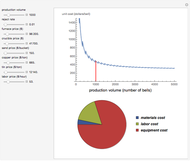
 Process-Based Cost Model for a Print and Copy Firm
Sam Shames -
 Band Structure of P-N Junction Semiconductor
Sam Shames -
 Crack Propagation and Stress Field for 2D Tensile Loads
Sam Shames -
 First-Order Solution to Glass-Ice Stefan Problem
Sam Shames -
 Crack Propagation for 2D Tensile Loading
Sam Shames