Primer on Bipolar Junction Transistors


Requires a Wolfram Notebook System
Interact on desktop, mobile and cloud with the free Wolfram Player or other Wolfram Language products.
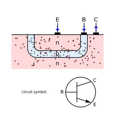
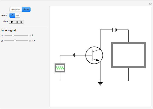
This Demonstration shows the operation of an npn bipolar junction transistor as a switch or signal amplifier. Most of the latest transistors, such as MOSFETs, are of the field-effect type, but junction transistors provide a simpler introduction to the basic concepts.
[more]
Contributed by: S. M. Blinder (September 2013)
Open content licensed under CC BY-NC-SA
Snapshots


Details
References
[1] Wikipedia. "Transistor." (Sept 5, 2013) en.wikipedia.org/wiki/Transistor.
[2] Wikipedia. "Bipolar Junction Transistor." (Aug 21, 2013) en.wikipedia.org/wiki/Bipolar_junction_transistor.
Permanent Citation
"Primer on Bipolar Junction Transistors"
http://demonstrations.wolfram.com/PrimerOnBipolarJunctionTransistors/
Wolfram Demonstrations Project
Published: September 11 2013
 Applied Voltage on an Ideal MOS Capacitor
Alberto Sottile Electrical Conductivity of Silicon Semiconductors
Nathan S Nelson Mechanism of a Solar Cell
Christopher P. Muzzillo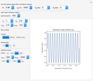 Synthesis of Rugate Optical Filter
Rodolfo Quintero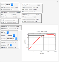 Small Signal (AC) Bipolar Parameters from SPICE Parameters
Allen Hollister Band Structure of P-N Junction Semiconductor
Sam Shames DC and AC Josephson Effects
S. M. Blinder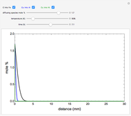 Diffusion in Solids
Nathan S. Nelson Series RLC Circuits
S. M. Blinder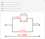 Effective Resistance of Network
S. M. Blinder
-
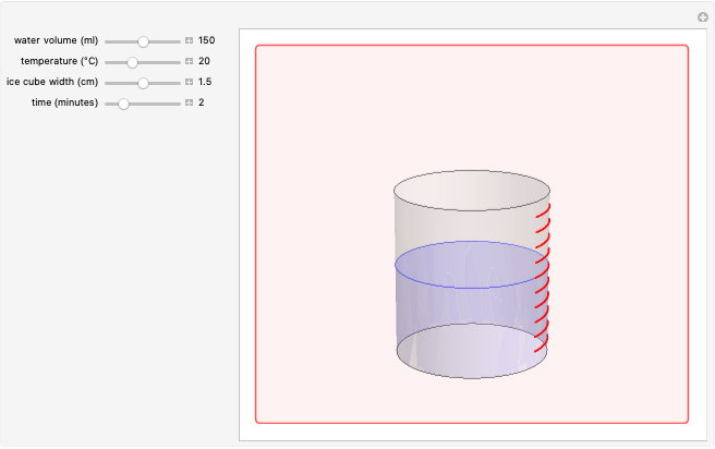 Ice Cube Melting in Water
S. M. Blinder -
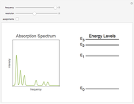 Absorption Spectroscopy
S. M. Blinder -
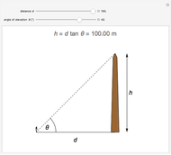 Height of Object from Angle of Elevation Using Tangent
S. M. Blinder -
 Internal Rotation in Ethane and Substituted Analogs
S. M. Blinder -
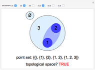 Topological Spaces on Three Points
S. M. Blinder -
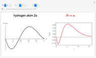 Hydrogen Atom in Curved Space
S. M. Blinder -
 Multipurpose Tool
S. M. Blinder -
 Statistical Thermodynamics of Ideal Gases
S. M. Blinder -
 Bell's Theorem
S. M. Blinder -
 Kepler's Mysterium Cosmographicum
S. M. Blinder -
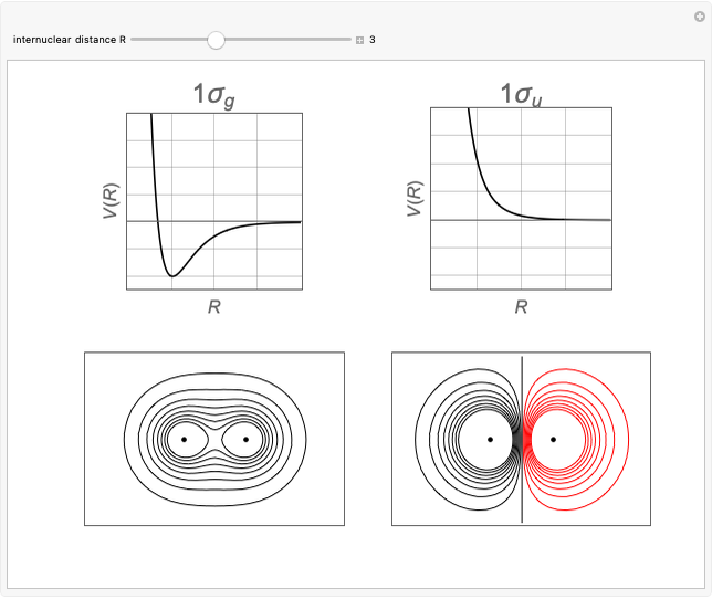 Bonding and Antibonding Molecular Orbitals
S. M. Blinder -
 Visible and Invisible Intersections in the Cartesian Plane
S. M. Blinder -
 Heron's Formula
S. M. Blinder -
 How Zippers Work
S. M. Blinder -
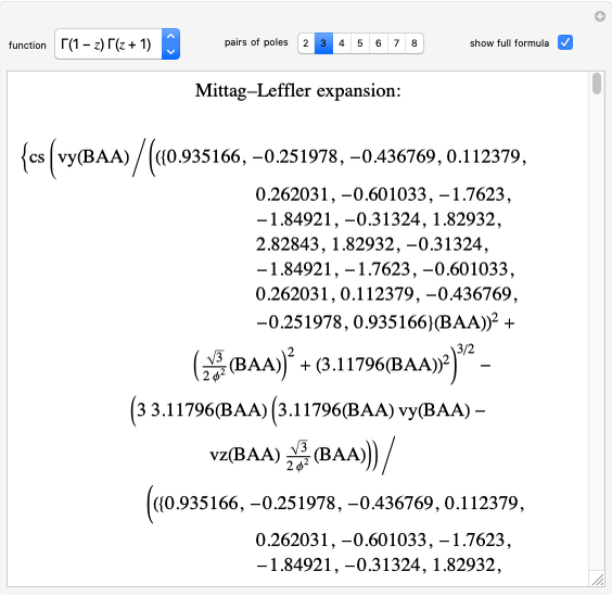 Mittag-Leffler Expansions of Meromorphic Functions
S. M. Blinder -
 Orbital Resonance in the Asteroid Belt
S. M. Blinder -
 Jordan's Lemma Applied to the Evaluation of Some Infinite Integrals
S. M. Blinder -
 Configuration Interaction for the Helium Isoelectronic Series
S. M. Blinder -
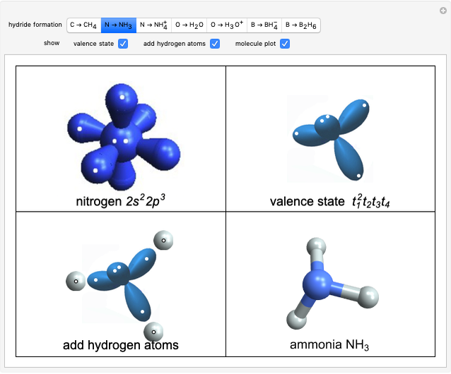 Structure and Bonding of Second-Row Hydrides
S. M. Blinder -
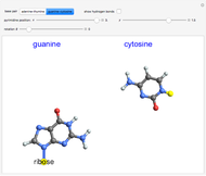 DNA Base Pairing
S. M. Blinder